Overview
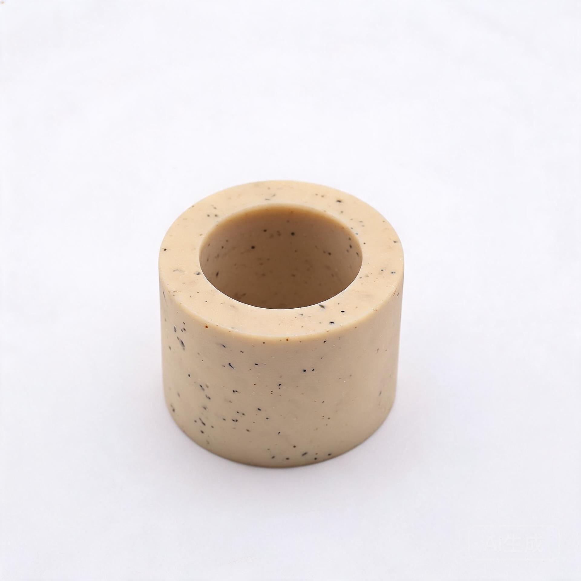
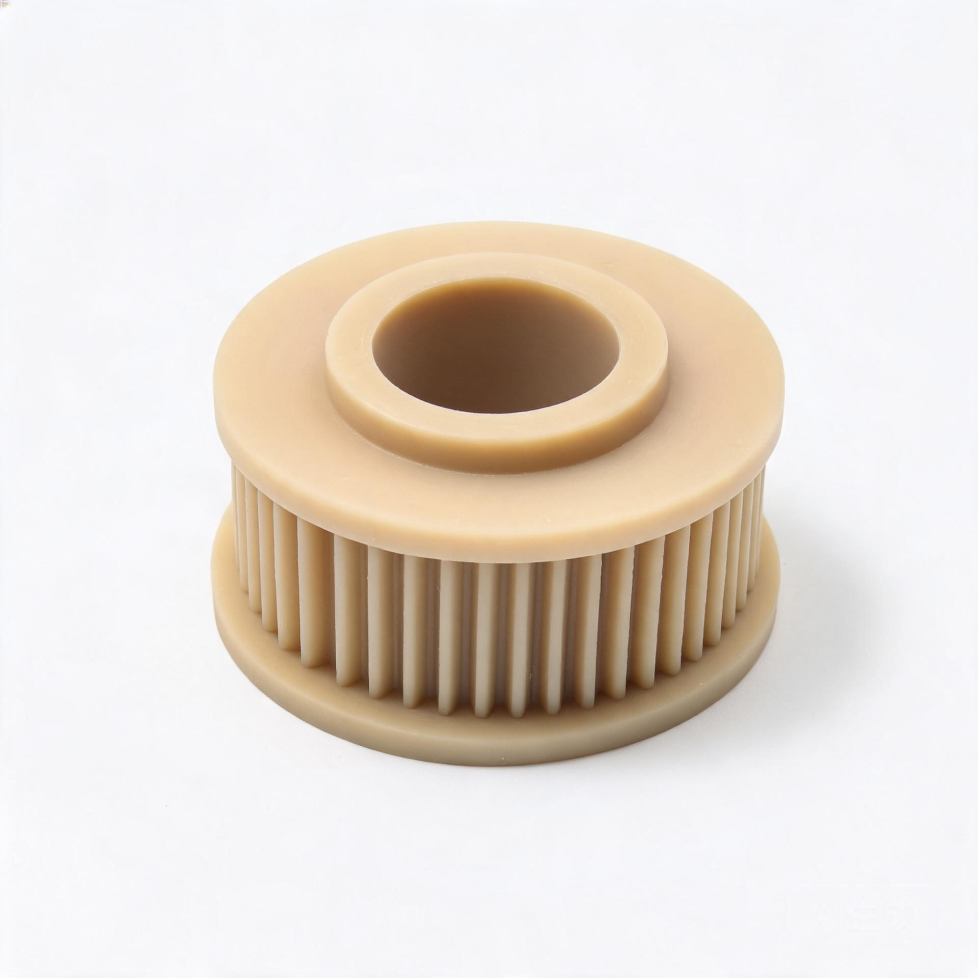
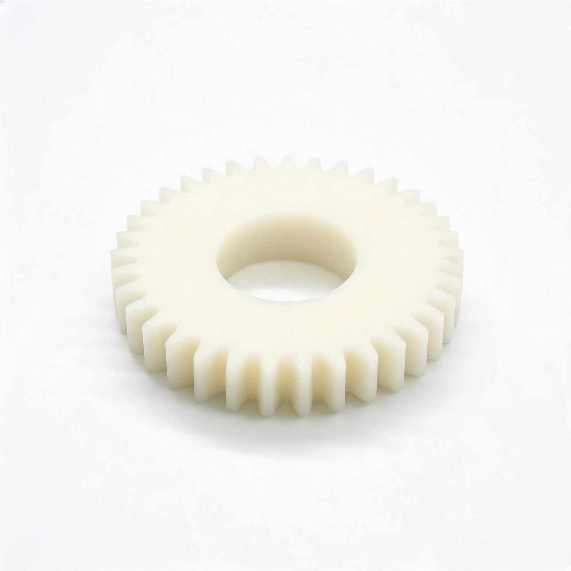
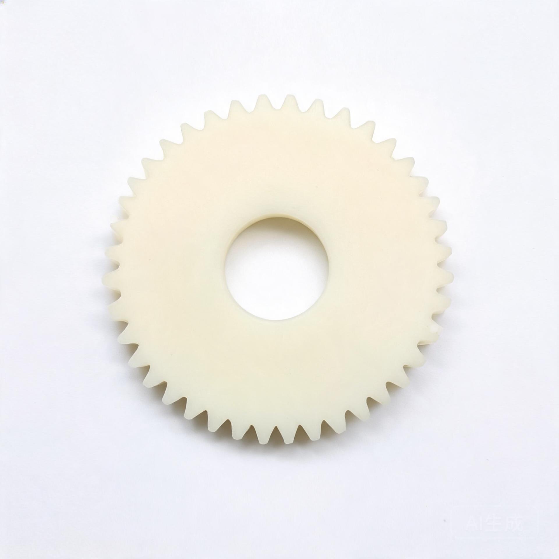
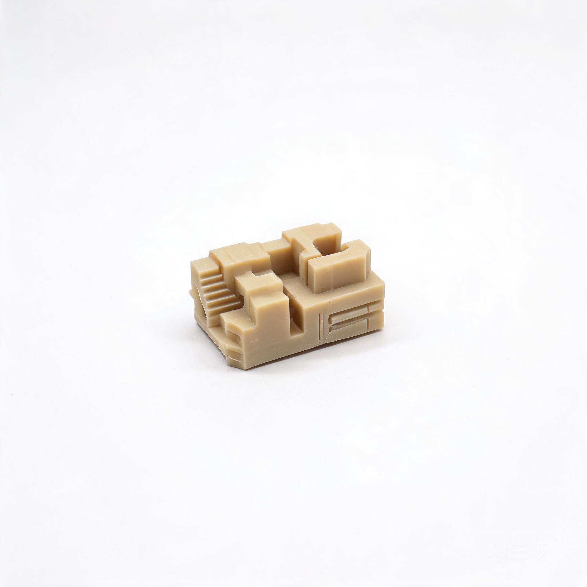
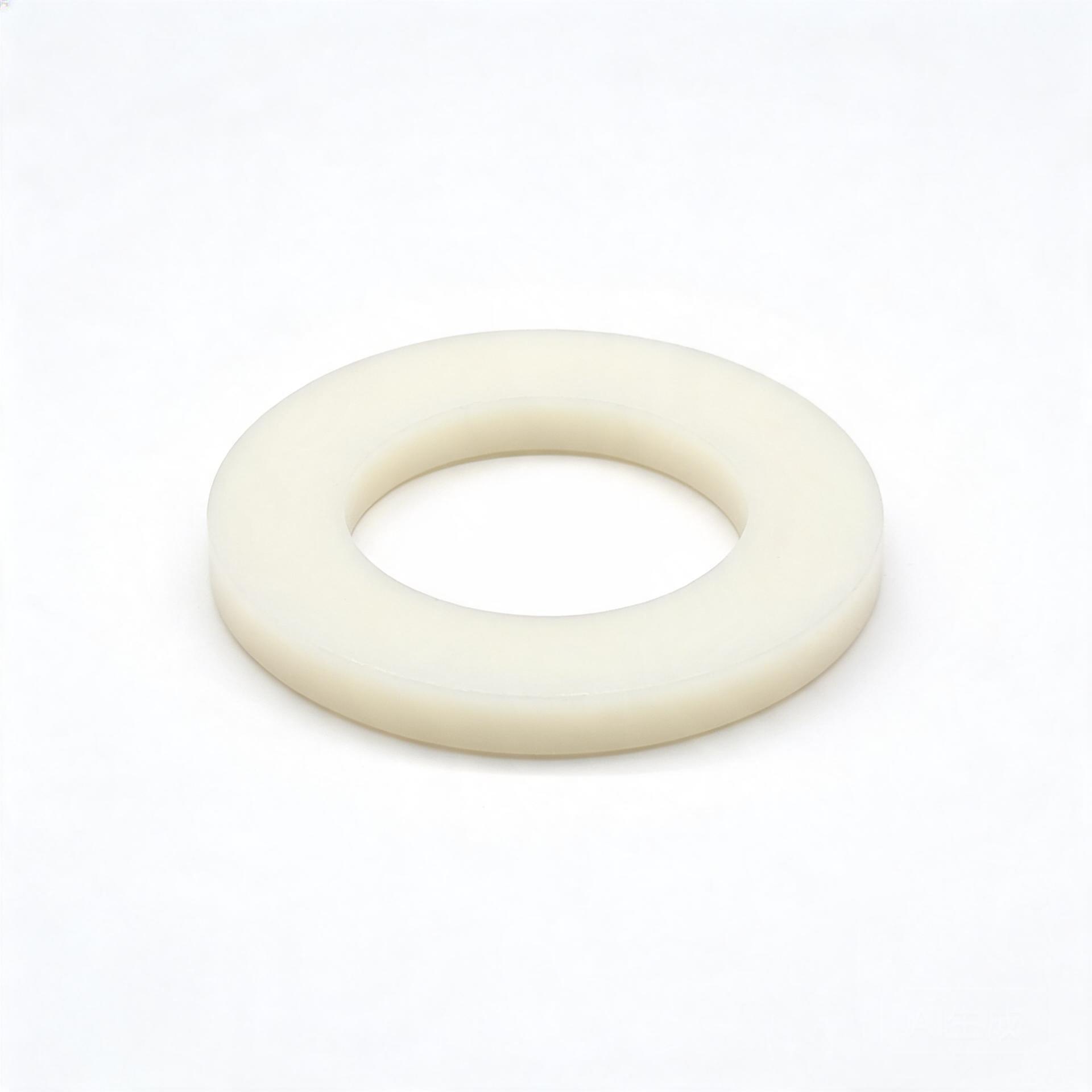
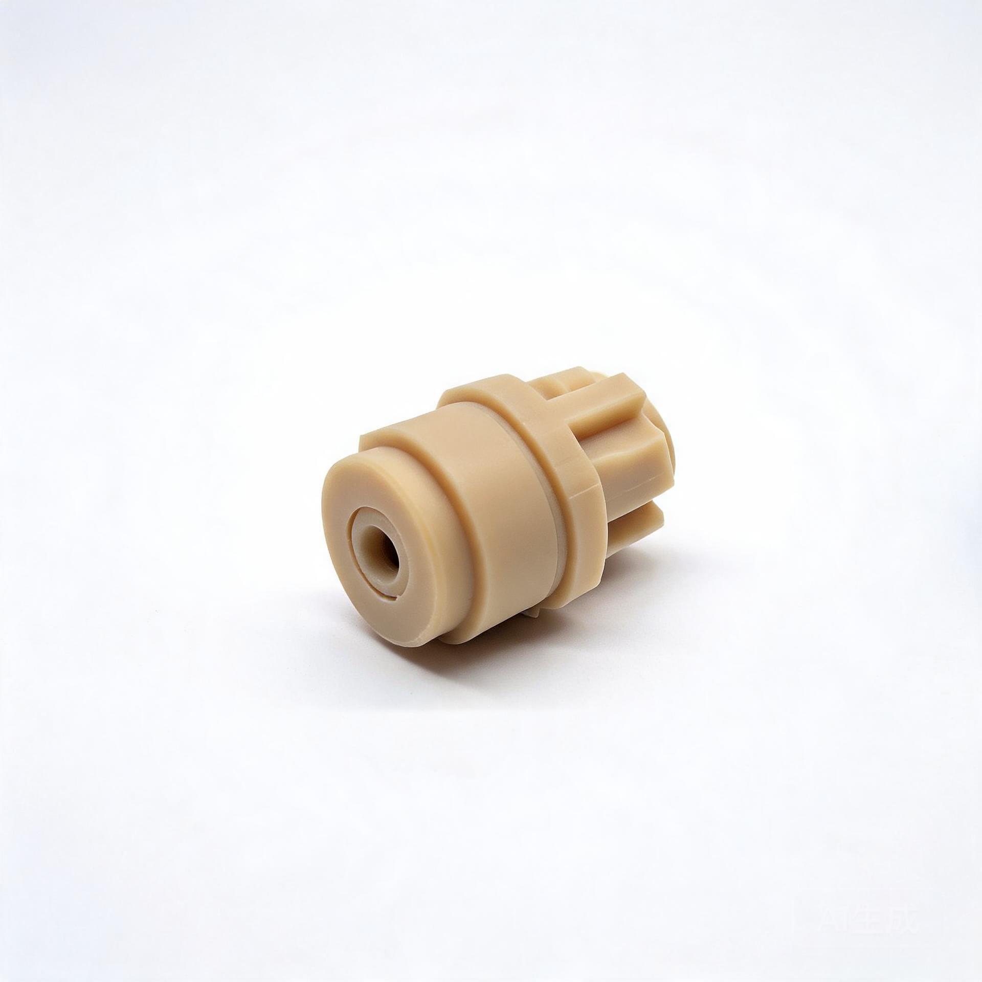
PEEK semiconductor insulators are high-purity insulating components machined from polyether ether ketone for use inside wafer processing equipment, where they isolate conductive parts, hold tight tolerances and must not shed particles or metallic contamination onto the wafer. Semiconductor-grade PEEK combines high dielectric strength with outstanding chemical resistance, low outgassing and thermal stability up to 260°C, making it suitable for plasma etch chambers, wet benches, ion implanters, metrology tools and wafer handling systems. OrroMFG produces PEEK semiconductor insulators by precision CNC turning, milling and 5-axis machining, with injection molding available for higher-volume insulator designs.
The critical advantage of PEEK in semiconductor service is that it delivers metal-like stiffness and creep resistance without the ionic contamination risk of metals and ceramics. Semiconductor-grade grades are produced with controlled extractable ion levels and low total mass loss, and are available in natural unfilled form for maximum dielectric performance or carbon-filled form for electrostatic discharge (ESD) control. PEEK resists the aggressive wet chemistries used in wafer fabrication, including hydrofluoric acid, sulfuric-peroxide mixtures and standard clean solutions, and it does not degrade under repeated plasma exposure. Our range includes chamber insulators, electrode standoffs, wafer chuck and lift pin insulators, gas line spacers, sensor housings, end effector pads and custom insulation geometries with tight concentricity and flatness requirements.
Key Features
- High Purity and Low Contamination: Semiconductor-grade PEEK is produced with controlled ionic extractables and low particle generation, protecting wafer yield in critical process steps.
- Excellent Dielectric Performance: Volume resistivity above 10¹⁵ Ω·cm and dielectric strength of 20-25 kV/mm provide reliable isolation in RF, plasma and high-voltage process equipment.
- High Temperature and Creep Resistance: Continuous service to 260°C with excellent dimensional stability under sustained load, so insulators do not relax or distort in heated chambers.
- Broad Chemical Resistance: Withstands hydrofluoric acid, sulfuric-peroxide mixtures, standard clean solutions, solvents and plasma chemistries that degrade most polymers.
- Low Outgassing and Vacuum Compatibility: Suitable for high-vacuum process chambers, with low total mass loss and condensable volatile content in qualified grades.
- ESD and Conductive Options: Carbon-filled PEEK grades provide controlled surface resistivity for static dissipation while retaining mechanical strength and thermal stability.
Material Specifications
| Property | Virgin PEEK (Semiconductor Grade) | 30% Glass-Filled PEEK | 30% Carbon-Filled PEEK | PEEK + PTFE Blend |
|---|---|---|---|---|
| Density (g/cm³) | 1.30 - 1.32 | 1.50 - 1.55 | 1.40 - 1.45 | 1.35 - 1.45 |
| Tensile Strength (MPa) | 90 - 100 | 120 - 140 | 130 - 150 | 70 - 85 |
| Tensile Modulus (GPa) | 3.6 - 4.0 | 7.0 - 8.5 | 7.5 - 9.0 | 3.0 - 3.5 |
| Flexural Strength (MPa) | 150 - 170 | 200 - 230 | 220 - 250 | 110 - 130 |
| Flexural Modulus (GPa) | 3.6 - 4.0 | 7.5 - 9.5 | 8.0 - 10.0 | 3.0 - 3.5 |
| HDT at 1.8 MPa (°C) | 150 - 160 | 230 - 250 | 240 - 260 | 140 - 155 |
| Continuous Service Temp (°C) | 260 | 260 | 260 | 240 |
| Hardness (Rockwell M) | 80 - 90 | 90 - 100 | 95 - 105 | 70 - 80 |
| Coefficient of Friction | 0.25 - 0.35 | 0.25 - 0.35 | 0.18 - 0.25 | 0.10 - 0.18 |
| Water Absorption (24h, %) | 0.10 - 0.20 | 0.10 - 0.20 | 0.05 - 0.15 | 0.08 - 0.15 |
| Dielectric Strength (kV/mm) | 20 - 25 | 15 - 22 | 12 - 18 | 18 - 24 |
| Volume Resistivity (Ω·cm) | 10¹⁵ - 10¹⁶ | 10¹⁵ - 10¹⁶ | 10³ - 10⁶ (ESD) | 10¹⁵ - 10¹⁶ |
| Outgassing (TML / CVCM, %) | < 0.5 / < 0.1 | < 0.5 / < 0.1 | < 0.6 / < 0.1 | < 0.5 / < 0.1 |
Applications
Semiconductor Manufacturing
PEEK insulators are used in plasma etch and CVD chambers, ion implantation equipment, wet benches, spin coaters, CMP tools and wafer transport robots. They isolate electrodes, gas lines, lift pins and sensor assemblies, and hold tight tolerances so that wafer handling repeatability is maintained. Low particle generation and controlled extractables help protect critical dimension yield on advanced nodes.
Electronics Manufacturing
In electronics production, PEEK insulators support test sockets, probe card fixtures, connector housings and high-frequency component holders for burn-in and final test. Their low dielectric loss and stable dielectric constant suit high-frequency and RF test environments, while heat resistance allows insulators to survive solder reflow and burn-in temperatures.
Medical Devices
Medical-grade PEEK insulators are used in surgical instruments, electrosurgical handpieces, implant tooling, sterilization trays and diagnostic equipment. PEEK is biocompatible, compatible with autoclave, gamma and EtO sterilization, and provides reliable electrical isolation in devices that must function after repeated sterilization cycles.
Analytical and Laboratory Instruments
Analytical instruments such as mass spectrometers, chromatography systems, ICP and spectroscopy equipment use PEEK insulators for probe housings, sample interface parts and electrode mounts. The material’s chemical inertness and low extractables prevent sample contamination, and its vacuum compatibility supports ion-source and detector assemblies.
Vacuum and High-Purity Systems
PEEK insulators are specified in vacuum feedthroughs, sputter targets, load-lock components and ultra-high-vacuum (UHV) chambers where low outgassing and thermal stability are essential. They resist plasma, ozone and reactive gas exposure without cracking or outgassing that would compromise chamber vacuum quality.
Operating Conditions
- Temperature Range: -40°C to +260°C (-40°F to +500°F) continuous; short-term excursions to 300°C with selected grades
- Voltage and RF Service: Suitable for high-voltage insulation and RF electrode isolation; dielectric properties remain stable from DC to microwave frequencies
- Vacuum Compatibility: Low outgassing makes PEEK suitable for high-vacuum and UHV process chambers when qualified grades are specified
- Chemical Compatibility: Resistant to hydrofluoric acid, sulfuric-peroxide mixtures, standard clean solutions, solvents, acids and bases; not recommended for molten alkali metals or elemental fluorine
- Plasma Exposure: Excellent resistance to oxygen, fluorine and chlorine-based plasma chemistries used in etch and deposition processes
- Mechanical Load: High compressive strength and creep resistance support sustained clamping loads up to roughly 100 MPa in well-supported insulator designs
- Particle and Cleanliness Requirements: Machined and cleaned to controlled particle and ionic contamination levels for cleanroom use
- Sterilization Compatibility: Withstands autoclave, gamma, EtO and electron-beam sterilization for medical and life-science equipment
Material Comparison
| Material | Purity / Outgassing | Temp Range | Mechanical Strength | Dielectric Strength | Cost | Best For |
|---|---|---|---|---|---|---|
| PEEK | Excellent (low TML/CVCM) | -40 to +260°C | Very High | Excellent | Very High | Chamber insulators, high-purity, high-temperature isolation |
| PTFE | Excellent | -200 to +260°C | Fair | Excellent | Medium-High | Inert wet-bench insulation, chemical lines, low cost vs PEEK |
| PPS | Good | -40 to +200°C | High | Good | Medium | Cost-sensitive insulators with moderate thermal load |
| Polyimide (PI) | Excellent | -200 to +300°C | High | Very Good | Very High | Extreme-temperature vacuum and cryogenic insulation |
| Alumina Ceramic | Excellent | -200 to +1000°C | Very High | Excellent | Medium-High | Very high temperature and wear, but brittle and heavy |
| Phenolic / FR4 | Fair | -40 to +150°C | Medium | Good | Low | General electrical insulation, panel and fixture parts |
Choose PEEK semiconductor insulators when:
- Ultra-low particle generation and controlled ionic extractables are required for wafer processing
- The insulator must survive HF, sulfuric-peroxide and plasma chemistries without degradation
- High-voltage or RF isolation is needed with stable dielectric properties
- Continuous service temperatures exceed the limits of PPS, phenolic and most other polymers
- Low outgassing and vacuum compatibility are essential for UHV process chambers
- ESD or conductive isolation is required and carbon-filled PEEK can be used
Customization Options
- Material Grades: Virgin semiconductor-grade PEEK, unfilled PEEK, 10-30% glass-filled, 10-30% carbon-filled (ESD), PEEK + PTFE blend, medical-grade and low-outgassing aerospace grades
- Component Types: Chamber insulators, electrode standoffs, lift pin and chuck insulators, gas line spacers, sensor housings, end effector pads, bushings and custom insulating profiles
- Size Range: From 3mm diameter insulators to parts over 300mm in diameter; turned lengths up to 500mm
- Tolerances: Machined to ±0.01mm on critical features and IT4-IT7 grade on mating diameters, with concentricity and runout controlled to 0.02mm
- Surface Finish: Sealing and sliding surfaces finished to Ra 0.2-0.8 µm; as-machined, tumble polished and deburred options available
- Cleaning and Packaging: Ultrasonic cleaning, DI water rinse, nitrogen dry and cleanroom double-bag packing for particle and ionic control
- Color and Identification: Natural amber, black (carbon-filled) and custom colors, with laser marking for part and batch identification
- Secondary Operations: Stress relief annealing, precision lapping, bonding, insert installation and assembly with mating components
- Design Support: Finite element analysis (FEA), tolerance stack-up review and prototype machining for new process tool designs
Quality Assurance
OrroMFG manufactures PEEK semiconductor insulators under an ISO 9001:2015 certified quality management system, with dedicated cleanroom production and handling areas for high-purity components. Incoming PEEK stock is verified by FTIR spectroscopy for polymer identity, DSC thermal analysis for grade confirmation, and mechanical property testing, while semiconductor-grade material is checked for extractable ion levels and outgassing data. All material is quarantined until released by the quality department and remains traceable to its production lot.
In-process inspection includes dimensional verification with coordinate measuring machines (CMM) and high-precision micrometers, together with concentricity, runout and flatness checks on critical insulating features. Surface finish is measured with profilometers, and finished parts are visually inspected for machining marks, embedded contamination and edge defects. Sampled insulators can be tested for dielectric withstand, volume resistivity and outgassing where the specification requires it. First article inspection (FAI) reports are produced for new part numbers and tooling, and each shipment can include a certificate of analysis (COA), dimensional inspection reports, cleanliness and particle data, and full batch traceability documentation. Cleanroom packing and lot segregation protect part cleanliness through to installation.